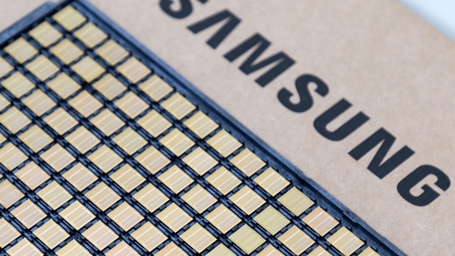
Samsung recently began mass production of sixth-generation high-bandwidth memory (HBM4) chips, becoming the first company in the world to do so. Now, the company is reportedly trying to accelerate production by introducing a cutting-edge semiconductor packaging technology at its chip plant in Cheonan, South Chungcheong Province, South Korea.
Samsung sets up HCB chip packaging equipment at its chip plant in Cheonan, South Korea
According to a report from New Daily, Samsung is establishing a Hybrid Copper Bonding (HCB) production line for HBM chips. This move is expected to shorten delivery times for HBM4 and future-generation HBM products (HBM4E and HBM5) for key clients such as Nvidia, while also reducing potential bottlenecks in the packaging process.
Equipment for the HCB line will arrive in March and will be used to set up manufacturing processes, run tests, and verify the quality of packaged chips. Once initial testing is successfully completed, full-scale production will begin. Samsung reportedly moved up its production schedule following requests from Nvidia.
What is HCB packaging for HBM chips?
HBM chips are built by stacking multiple layers of memory dies vertically. As the number of layers increases, the chip becomes thicker and generates more heat, making efficient cooling essential. Because of this, chip packaging must also evolve to better manage thermal load and electrical stress.
Hybrid Copper Bonding improves the physical and electrical connections between stacked layers. At a recent industry event, Samsung’s technical chief said the HCB process could reduce thermal resistance by up to 20 percent. However, industry observers caution that performance gains demonstrated in laboratory conditions do not always translate directly to mass production, where yield, reliability, and cost efficiency become critical.
HBM chips are getting more complex
Until now, companies such as Micron, Samsung, and SK hynix have mainly competed on core HBM specifications, including data transfer speed and total memory bandwidth. As HBM technology grows more complex with each generation, additional factors such as heat management, power efficiency, manufacturing yield, and production stability are becoming increasingly important.
The broader semiconductor industry is watching closely to see how quickly Samsung can establish its HCB packaging line and how effectively its HBM4 chips perform when paired with next-generation AI accelerators such as Nvidia’s Rubin and AMD’s MI450.
The post Samsung is trying to boost HBM4 chip production for Nvidia appeared first on SamMobile.


 Loading ...